Challenges of an Electronics Engineer
2024-04-02
Post by: Thomas Bui

The description of what an Electronics Engineer does at Axis is quite simple. We begin by drawing a schematic. From that schematic, circuit boards are ordered with all the necessary components soldered. Lastly, when the circuit boards arrive, testing are done to verify that all components are functional and operating within specification. And that’s it, simple, right?
Well, one could only wish for things to go that smoothly. As you all know, nothing will ever work the first time. It is the same thing here at Axis, and it’s weirdly the best part of the job, which is facing the challenges of the problems. Problems are the best way of learning and a perfect opportunity for creativity.
This blog post will not focus on the problems faced at Axis as an Electronics Engineer. Instead, this post will give a quick overview of some areas where we often face problems.
Schematic design
As an Electronics Engineer at Axis, when we draw our schematics, much of it originates from well-tested reference designs made by other electronics engineers here at Axis. This is both to ensure that all projects follow the high quality standards set by Axis and to save time when developing new products. We do not want to reinvent the wheel, we just want to improve and develop new things.
Even though much of it is copy-pasting, you still need to have a deep understanding of the schematics and how to integrate your own design with the existing reference designs. The common issues in the schematic process could be small, like a non-connected trace, or something as big as having the wrong power source to the CPU.
That is why we have a schematic review. Schematic review means that some of your colleagues with relevant competence review your design. This ensures that we don’t miss small details, often invisible to the designer’s eye.
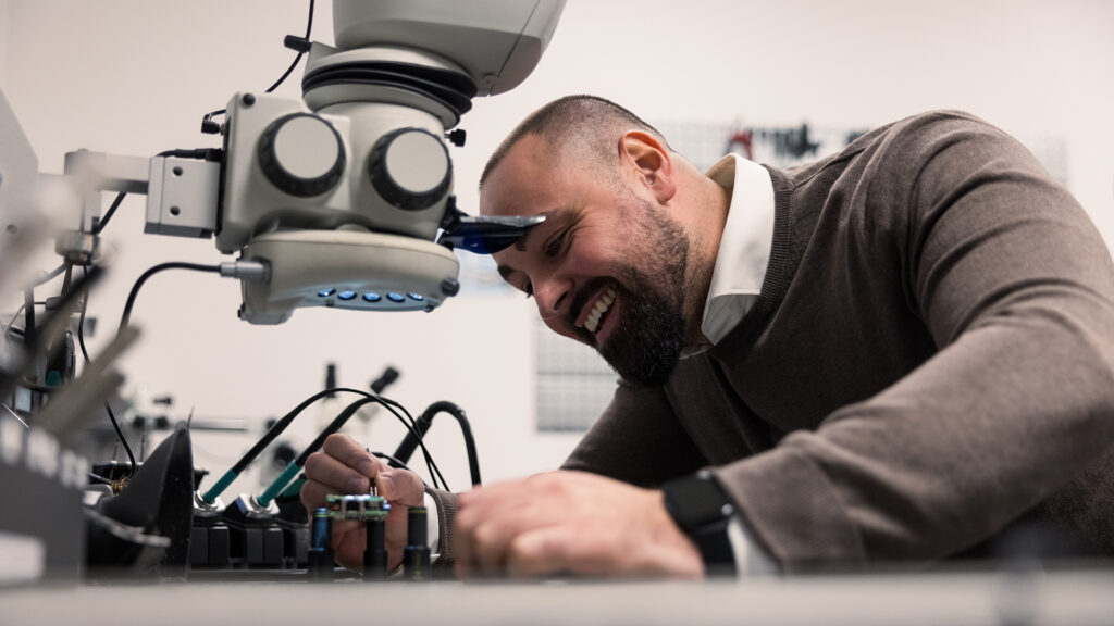
Measurement setup
After the schematic review, a circuit board is drawn up by one of our CAD engineers and ordered with components soldered on. When they arrive, different types of evaluations are done to ensure functionality and compliance with the standards set by different countries.
The types of measurements vary, from testing the quality of the power voltage and data signals to evaluating how the product handles extreme temperatures. However, when you test and observe the behavior of the unit, there will always be an influence that affects the results differently depending on your measurement setup. And the key is to find a method that influences the result as little as possible.
One example is when we use probes to measure voltage ripples, which is a way to determine the quality of the voltage. The results vary depending on how big your loop area is. The loop area is the physical length between the tip of where you measure to the end of your ground cable, meaning that the shorter the cables, the smaller the loop area. The loop area works as an antenna and can pick up surrounding noise that has nothing to do with the actual signal measured, resulting in non-reliable results that may appear worse than they really are. This is one of many examples of how the measurement setup affects the result negatively.
So, our job is to together with all electronic engineers at Axis find and agree on a method that ensures reliable results.
EMC
One compliance test that we do both in-house and at a third-party company is Electromagnetic Compatibility (EMC). EMC characterizes a device’s interaction with its surroundings without impacting its own functionality but also the functionality of other devices. There are many subtests that evaluate EMC, but I‘ll briefly cover the ones Axis evaluates and certifies.
During EMC certification, we examine how much emission the device emits, which can both be in the form of radiated and conducted. Additionally, we assess how effectively a device protects itself from surrounding emissions. These emissions come in the form of radiated, conducted, Electrostatic Discharge (ESD), burst pulses, and surge pulses.
Let’s delve into radiated emissions and radiated immunity. Essentially, all conducting material with a current flowing through it radiates electromagnetic waves at different frequencies. These waves can induce and generate unwanted energy in a recipient device and potentially impact the functionality or even cause damage. Radiated immunity is the opposite of radiated emissions, and that is how well we can protect our devices from being impacted negatively by unwanted emissions from surrounding devices.
Moving on to conducted emissions and conducted immunity. Conducted emissions are unwanted noise generated from your device that may leak out to other connected devices or subcircuits through for example cables and Printed Circuit Board (PCB) traces. Conducted immunity is the opposite, and that is how well we can protect our own device from unwanted noise generated and transferred from other devices through cables and PCB traces.
The third immunity test is ESD. The purpose of the ESD test is to evaluate how well your device and its components are at withstanding, as the name implies, electrostatic discharges that can build up in for example, humans and inside the device.
The fourth immunity test is burst. The characteristics of burst pulses are high repetitive, low energy pulses with a short rise time. These pulses can result from changes in for example inductive loads. One example is if a motor is running smoothly and is abruptly stopped, there will be a short burst pulse generated. This can impact the functionality of the device, such as flicker noise on the resulting image.
The last immunity test is surge, which protects against momentary high energy level pulses such as lightning. We have a machine capable of generating up to 8000 volts, this is to emulate surge pulses.
So, to summarize, our job as an electronic engineer is to suppress emissions and increase the immunity of our devices.
Final words
The curiosity for understanding the world around us it’s the reason why engineers studied what they do. And the best way to learn and understand something is not by lectures at the university, but by doing and facing those challenges yourself and find your unique ways together with the help of other and solve them.